
Non Volatile Technologies Pty Ltd
BALLINA AUSTRALIA 2478 (ABN 96 078 508 264) Ph:+61 2 9016 4695
"Helping others to have a future assures our own."
- Home
- Past Projects
Plasma Reactor
Non Volatile Technologies Pty Ltd
BALLINA AUSTRALIA 2478 (ABN 96 078 508 264) Ph:+61 2 9016 4695
"Helping others to have a future assures our own."
Plasma Reactor
|
Plasma Reactor for Depositing Thin Polymer Films to Make Capacitors 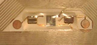
Fig 1. Ceramic Chip Capacitors and BagTag ASIC
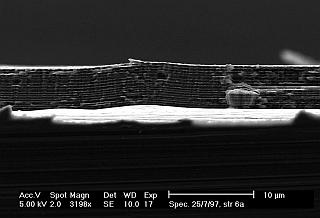
Cross-section of a capacitor cut with a laser
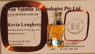
Working Model - Thin Film Capacitor connected to a BagTag
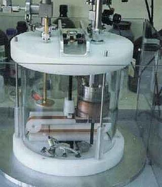
Fig 4. Prototype Plasma Reactorn-1996 Ian Wark Laboratories
Introduction From 1993 to 1997 I was involved in a project, the aim of which was to develop RFID technology suitable for use in airline baggage labels. It was, by any measure, an ambitious project. The technology was based on an RFID transponder that utilised a new type of Ferro-Electric Non Volatile Memory (called FRAM™) and was powered at 132kHz. The transponder broadcast its signal on 32 different frequencies randomly from around 1MHz to 30MHz with a data transfer rate of around 100kBits/Second. To do this required two antennae; one for powering and one for transmission. The silicon chip (called an Application Specific Integrated Circuit - ASIC), comprising the transponder, required there be two capacitors; one 5.6nF and one 330nF. (See Figure 1) The smallest temperature stable ceramic chip capacitors I could find were from a company called Novacap founded by Dr Andre Galliath (a truly exceptional person, on many levels, I'm pleased to call a friend). As thin as Novacap's capacitors were, they still made incorporation of the RFID device into labels and credit cards a challenge. Being ceramic, they were also susceptible to damage. In 1994 I learnt about work the CSIRO had done laying down ultra-thin, polymeric films in a plasma for the purposes of placing a coating on long-wearing contact lens. Before approaching the CSIRO, I filed for a provisional patent describing how it was possible to manufacture ultra-thin (and hence flexible), high value, temperature stable capacitors to a precise value. The CSIRO already had some experience in laying down polymers in a plasma using hexa-methyl-di-siloxane as the monomer to coat the surface of contact lenses so as to make them suitable for extended wear by users. My idea was to sputter silver, copper, aluminium, platinum or gold down between a mask. After laying down the metal, a broader mask would be employed to lay down a thin layer of HMDSO.One of the materials they used was hexa-methy-di-siloxane (HMDS0). HMDSO was significant because it contains silicon and therefore had a higher dielectric coefficient than compounds that were purely organic. (My eventual aim was to find a monomer that incorporated a titanate, such as Tetrabutyl Titanate, and therefore would yield a higher dielectric constant.) The concept of laying down ulta-thin films attracted my attention for the following reasons:
Personalities at the CSIRO When making contact with the CSIRO, I met with Dr Albert Mau, the person heading that Division. He introduced me to Dr Hans Griesser, the person who had been active in the field of plasma polymerisation for some time. When approval for the project was given by the Board of Intag, I was introduced to Dr Robert Fleming, a physicist who, like myself, had an interest in plasma polymerisation. The lab technician who built the reactor was Zoran Vasic. Zoran was particularly useful in that he required very little direction and exercised his initiative on many occasions. I really only had to sketch out my concepts and Zoran turned them into a functioning reality.A Snapshot of what was achieved Figure 2 shows a micro-photograph of capacitors made, using the process I had conceived, at the Ian Wark Laboratories, Clayton, Victoria with the help of the CSIRO's Division of Chemicals and Polymers.Figure 3 is a picture of an actual thin film capacitor that was made using the processes we developed and which worked as a tuning capacitor on a BagTag ASIC. Figure 4 is a picture of the Plasma Reactor that was built to my design by Zoran Vasic. A Primer on Polymerisation in Plasma A Plasma is created by having a highly evacuated space into which a small portion of a gas such as Argon is inserted and a high voltage is put across two parallel plates separated by some distance. The effect of doing this is that electrons flow from the negatively charged plate to the positively charged plate using the gas molecules as their "stepping stones". When this happens the space will glow with light of a frequency related to the gas that is providing the stepping stones for the electrons.If you then inject into this highly evacuated chamber a monomer, the electrons travelling from one plate to the other collide with the molecules of monomer, knocking electrons off them and causing the creation of points on the molecule that want to bond with other similarly affected molecules. (These areas are called "active polar groups".) When these monomer molecules combine with other activated monomer molecules, the form a polymer (many monomer molecules now chained together). As the polymeric molecules form, they precipitate out the gas and fall towards earth, landing on whatever surface is below. The layers formed are very thin (as in nanometres) but because the molecules are still very active, they continue to chain together as they lay on the surface; joining up any holes that may be present. This results in a hyper-crosslinked plastic membrane that is free from pin-holes. In the case of HMDSO, if a high voltage was used to cause the plasma, the material that landed on the surface contained a higher percentage of silicon. This meant it had superior dielectric properties. Next the hyper-crosslinked nature of substances meant they would have mechanical properties far superior to what was possible in a normal chemical reaction. This had the promise of making plastic substances that could withstand high temperatures and would have significantly superior tensile strength. Highly cross-linked molecules were also known to exhibit an very good memory and as a consequence high resistance to permanent deformation. |
|
Concept for Fabricating Capacitors 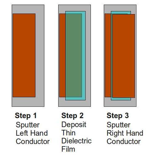
Fig 5. Process used to fabricate a capacitor. |
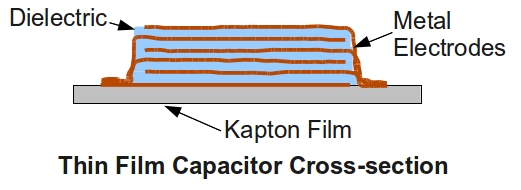
Fig 6. Cross-section of a Thin Film Capacitor
|
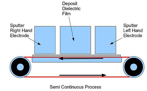
Fig 7. Process to fabricate capacitors on a continuous band |
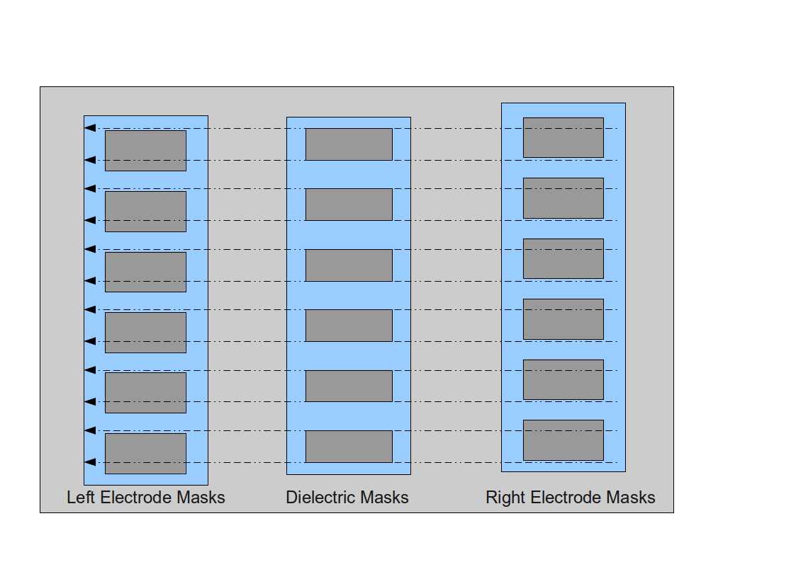
Fig 8. Creating multiple strips of capacitors |
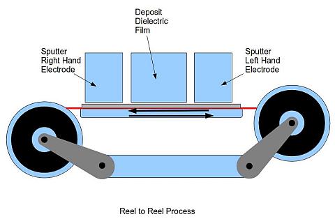
Fig 9. Volume production of capacitors using a reel to reel process |
|
Cutting the Capacitor Tape to Create Individual Capacitors 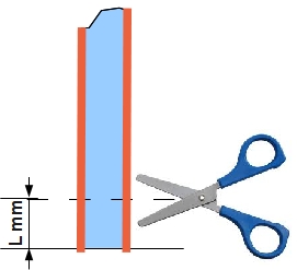
Fig 10. Cutting off capacitors to achieve a set value
Cutting the Tape In order to create individual capacitors it is necessary to cut the tape and to seal off the edges of the cut. When the tape is cut into segments, each segment consists of a left and right electrode and two cut edges which have most probably been traumatised by the cutting action. From the outset, it was appreciated that, with cutting, there was the possibility of smearing of metal from one electrode to the next. This would result in short-circuiting the capacitor. One simple way of possibly solving this would be to apply a high current to the circuit in an oxygen-rich atmosphere and simply burn the metal, turning it into a non-conducting oxide. Cutting the capacitor and the treatment of the cut edges became one of the more challenging aspects of this project. It was never properly resolved due to the project being terminated because of a lack of funds and the unwillingness of the Intag Board to proceed with further R&D.;Achieving Precise Values Producing the capacitors in a tape then enables the creation of capacitors to a precise value with minimal wastage. Because the tape has a reasonably consistent value of capacitance per unit of length, it is possible to cut the tape to a particular length, measure the resulting capacitance, and then make an adjustment to the length of the next cut to ensure that the value derived is absolutely precise. In this manner, it is believed it would be possible to produce capacitors to +0.1% accuracy (See Figure 10.) |
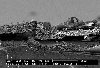
Fig 11. Result of cutting with sharp scissors
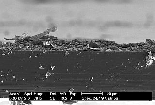
Fig 12. Result of cutting with a Diamond Knife
Minimising Wastage A by-product of achieving high levels of precision in the manufacture of this type of capacitor is that one also has little wastage. The accuracy achieved by this method of production is far superior to that which is possible with ceramic chip capacitors. For example, it is normal when making ceramic chip capacitors for up to 30% of the capacitors not to fit within the desired tolerance. The tighter the tolerance, the greater the wastage. When that happens, those capacitors that fail badly are likely to fit into the tolerance band of another value of capacitor. Where that is not the case, the capacitors are retained in the store, in the hope of satisfying a special order where the customer does not want a standard value.Cutting Methods The method used to cut the tape is not only fundamental to the successful operation of the capacitor but also will determine, to some extent, the wastage. Shearing the tape using, for example, a scisors or cutting action involves virtually no wastage at all but unfortunately, experiments indicated that, even with a diamond knife(as can be seen in Figures 11 and 12), the results of this type of cut were not good. |
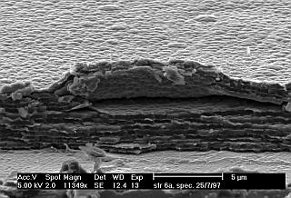
Fig 13. Result of cutting with Water Jet.
Fig 14. Result of cutting with laser ablation technique.
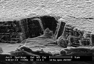
Fig 15. Highly Magnified view - |
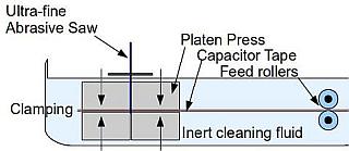
Fig 16. Capacitor held between platens in order to micro-saw 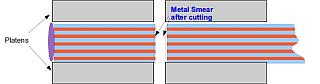
Fig 17. Capacitor held between platens just after saw cut 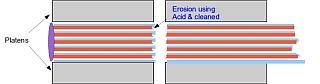
Fig 18. Capacitor after acid wash to clean up metal smearing 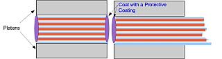
Fig 19. Protective coating applied to the treated edge Experimentation Experimentation took the form of firstly, manually creating single capacitors through a mask. The second step was to have a travelling tape and lay down alternate layers of polymer and metal using plasma polymerisation and sputtering. Of interest, it was possible with some adjustments to conduct both operations in the same chamber at the same time. It was also found that, as one increased the energy of the plasma, the HMDSO's composition became more heavily biased towards silicon. The other interesting phenomena observed was that the plastic film had mechanical properties far superior to those possible with a normal chemical reaction. For example, the tensile strength of the finished product was around 7 times that of "normal" silastic. The maximum temperature the substance could withstand was also considerably greater, being around 240C as opposed to 110->125C.Interesting Possiblities for Additional Research This work led onto the means of creating armour plate from micro-layers of polymer and amorphous diamond. Because the resultant polymers are hyper-cross-linked, the process also has potential for the creation of super micro-fibres for use in highly specialised textiles. |